Intel is already using ASML’s High NA EUV technology on selected layers of some Panther Lake processors, according to ASML’s July 15, 2026 announcement. The next question is how far this optical approach can keep pushing chip patterns before the machinery needs a more fundamental change.
Hyper NA EUV lithography is one proposed answer. It would increase the numerical aperture of the optics from 0.55 to at least 0.75. The ambition is finer patterning while preserving much of the existing EUV ecosystem. A 2025 conference abstract by ZEISS engineer Michael Patra describes that direction; it does not establish a production-ready scanner.
Why Hyper NA EUV lithography keeps the same light
A lithography machine projects a circuit pattern from a mask onto a wafer coated with light-sensitive material. Its optics reduce and focus that pattern, rather like an exceptionally precise projector. ASML explains the projection process here.
Smaller printable details depend on wavelength, numerical aperture and the manufacturing process. Raising the aperture lets the optical system capture a wider angular range of light. That offers a way to improve resolution without immediately changing the wavelength, as ASML’s explanation of the Rayleigh criterion shows.
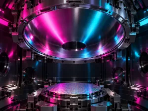
High NA already uses 13.5-nanometer EUV light, with aperture 0.55. ZEISS describes its projection optics as roughly 12 tons and more than 40,000 parts. The scale of that hardware is the striking counterpart to the tiny structures it helps produce. ZEISS’s technical overview explains the mirror system.
The five-nanometer number needs context
Patra’s abstract identifies optical resolution limits of 13 and 8 nanometers half-pitch for existing EUV scanner families, then describes a next generation approaching 5 nanometers half-pitch. Half-pitch is half the repeat spacing of a regular pattern. It is an optical patterning measure, not a promise that every transistor dimension—or a chip’s advertised process-node name—will equal five nanometers.
The same abstract says Hyper NA’s mirrors would grow significantly, while the machine footprint would barely increase. Larger optics do not automatically mean a proportionally larger space requirement in the factory. That is a design proposition, not a measured specification for a commercial Hyper NA tool.
A sharper pattern still has to survive manufacturing
Patra identifies two commonly discussed risks: three-dimensional effects at the mask and polarization effects at the wafer. Both concern how light behaves through the imaging system. The conference contribution outlines the issues and planned mitigation discussion, rather than proving they have been solved in mass production.
The practical test is therefore broader than an impressive resolution number. Manufacturers need patterns that can be repeated reliably and integrated into usable chips. High NA’s selected-layer production milestone supplies evidence for today’s technology; Hyper NA still needs its own manufacturing evidence. For readers watching the chip race, that distinction separates a promising optical route from a machine ready to earn its place on a factory floor.