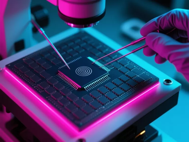
Engaging with hardware can be a rewarding experience, especially for those with a background in software development. This article recounts the journey of designing and assembling a custom PCB for a BME280 sensor module, showcasing the steps taken and the tools used.
The Initial Steps
A couple of months ago, the author acquired an Arduino Nano ESP32 development board, sparking an interest in hardware experimentation. Despite limited experience in hardware, the author quickly managed to blink built-in LEDs using the Arduino IDE and assistance from large language models (LLMs). This initial success led to a desire to build and flash firmware directly from the command line, which further boosted confidence in returning to familiar coding tools.
From Prototyping to Production
After experimenting with the Arduino board, the author sought to move beyond prototyping. The goal was to create a more permanent solution by designing a custom PCB for the BME280 sensor. The BME280 sensor, which measures temperature and humidity, was chosen for its simplicity and the potential for a plug-and-play implementation.
Designing the Schematic and PCB
For the PCB design, the author selected KiCad, a free and open-source software, to create the schematic and layout. The design process began with referencing the BME280 datasheet, which provides essential information such as pin configurations and connection diagrams. The author opted for an I2C interface to facilitate communication between the sensor and the ESP32 chip.
While KiCad is not the most intuitive tool for beginners, the author successfully created the schematic and then transitioned to the PCB layout. This involved selecting appropriate footprints for the components, which dictate the board’s size and assembly ease. The author chose 0805-sized SMD components for their suitability for hand soldering.
Component Sourcing and Assembly
Components were sourced primarily from DigiKey, although the BME280 sensor was unavailable, prompting the author to repurpose one from a previously purchased module. After generating a bill of materials (BOM) in KiCad, the author exported the necessary gerber and drill files to order the PCB from JLCPCB, which took about 2-3 weeks and cost under $10.
The assembly process involved desoldering the BME280 from the Amazon module, applying solder paste, and carefully placing the components. Despite initial concerns about potential short circuits, the assembly was successful on the first attempt, with the custom board functioning as intended without firmware modifications.
This project provided valuable insights into the PCB design and assembly process, paving the way for more complex projects in the future.
This article was produced by NeonPulse.today using human and AI-assisted editorial processes, based on publicly available information. Content may be edited for clarity and style.
Original source: vilkeliskis.com